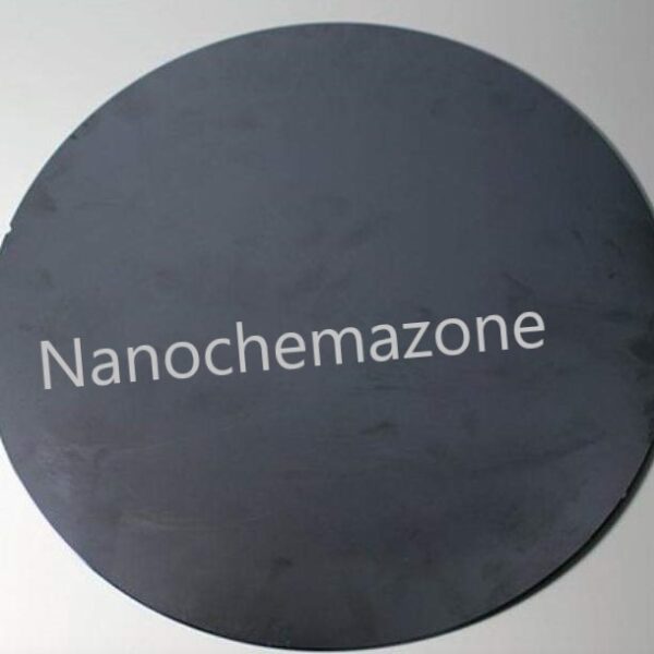
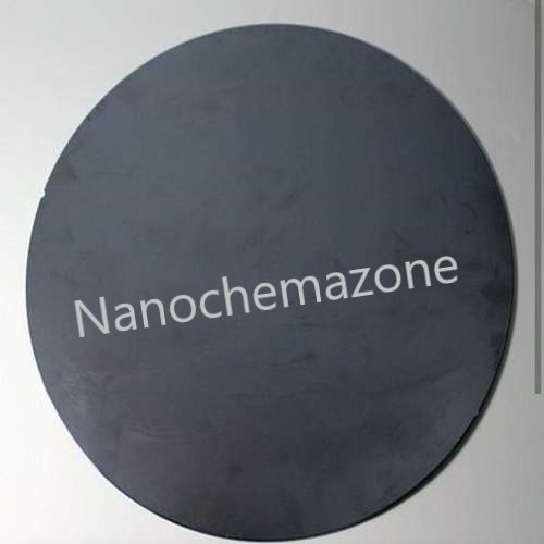
Single Crystal Silicon Wafer N-Type (1 inch)
Product Name: Single Crystal Silicon Wafer N-Type (1 inch)
| Product Name |
Single Crystal Silicon Wafer N-Type (1 inch) |
| Cat No. |
NCZ-NSC330/20 |
| Size |
1 inch |
| Thickness |
300-380 micro-meter |
| Type |
N-type |
| Dopant |
Phosphorus |
| Resistivity |
1-10 ohm/cm |
| Surface |
Single side polished |
| Boling Point |
2355 °C (lit.) |
| Melting Point |
1240 °C,1410 °C (lit.) |
| Density |
2.33 g/mL at 25 °C (lit.) |
| Semiconductor Properties |
<100>, N-type |
| SMILES string |
[Si] |
Physical properties:
0 vortex defects. Etch pitch density (EPD) < 100 (cm-2). Resistivity 100 – 3000 Ωcm.
Oxygen content: ≤ 1~1.8 x 10¹⁸ /cm3; Carbon content: ≤ 5 x 10¹⁶ /cm3; Boule diameter: 1~8 ″
Description:
Single Crystal Silicon Wafer N-Type (1 inch). We have heated polished doped single-crystal silicon wafers in a single-mode microwave cavity to temperatures where surface to surface bonding occurred. The absorption of microwaves and heating of the wafers is attributed to the inclusion of n-type or p-type impurities into these substrates.
A cylindrical cavity TM (sub 010) standing wave mode was used to irradiate samples of various geometry at positions of high magnetic field. This process was conducted in a vacuum to exclude plasma effects.
This initial study suggests that the inclusion of impurities in single crystal silicon significantly improved its microwave absorption (loss factor) to a point where heating silicon wafers directly can be accomplished in minimal time. Bonding of these substrates, however, occurs only at points of intimate surface to surface contact. The inclusion of a thin metallic layer on the surfaces enhances the bonding process.
Please email us for the customization.
Email: contact@nanochemazone.com
Please contact us for customization and price inquiry
Note: We supply different size ranges of Nano and micron as per the client’s requirements and also accept customization in the various parameters

")