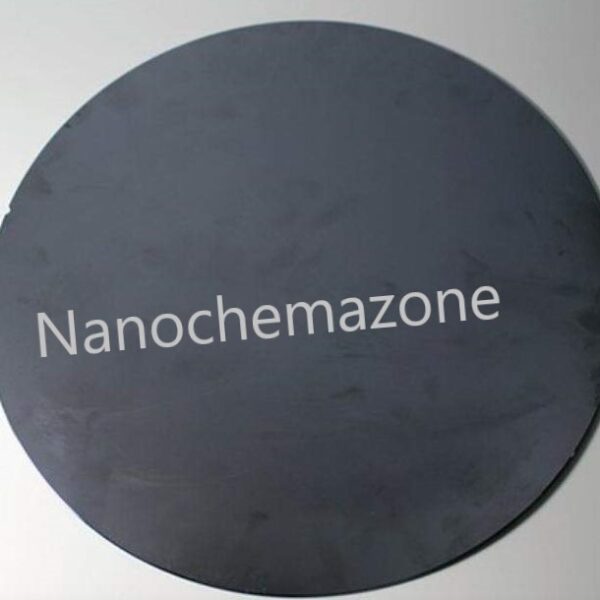
Single Crystal silicon-silicon dioxide Wafer
Product Name: Single Crystal silicon-silicon dioxide Wafer
| Product Name |
Single Crystal silicon-silicon dioxide Wafer P-type (4 inches) |
| Cat No. |
NCZ-NSC318/20 |
| Día |
100 mm (4 inches) |
| Orientation |
<100> |
| Wafer thickness |
500 micrometer |
| Resistivity |
<0.01 |
| Polished |
Front Side Polished |
| Thickness |
300 nm (dry) |
| Purity |
99.9% |
| Formula |
Si/SiO2 |
Provided in a single wafer case
Silicon oxide wafer SIO2 thin-film among semiconductor technology, SiO2 thin film layers are mainly used as dielectric material and more recently, they are integrated with MEMS (Micro Electro Mechanical Systems) devices. The simplest way to produce silicon oxide layers on silicon wafers is to oxidize silicon with oxygen.
Single Crystal silicon-silicon dioxide Wafer RELATED INFORMATION
Storage Conditions:
Airtight sealed, avoid light and keep dry at room temperature.
Please email us for the customization.
Email: contact@nanochemazone.com
Note: We supply different size ranges of nano and micron size powder as per the client’s requirements and also accept customization in various parameters.

")