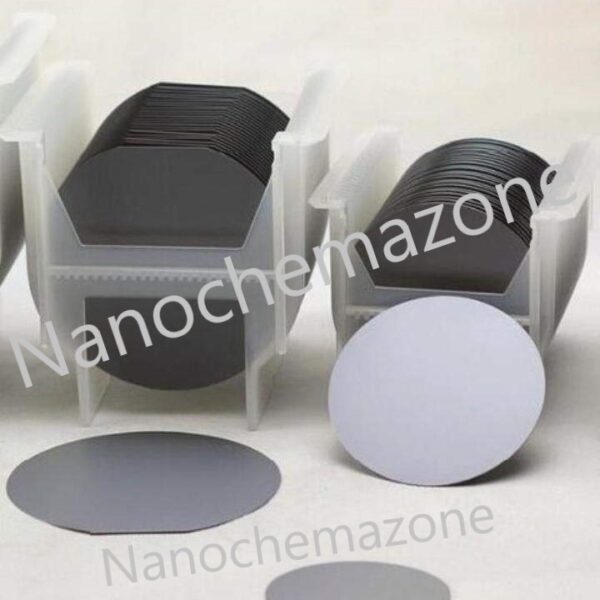
Product Name: Single Crystal silicon-silicon dioxide Wafer N-type (4 inches)
| Product Name: |
Single Crystal silicon-silicon dioxide Wafer N-type (4 inches) |
| Cat. No. |
NCZ-NSC 326/20 |
| Diameter |
100 mm (4″) |
| Product Name |
Silicon Oxide Wafer |
| Oxide Thickness |
100 nm (dry) |
| Color |
Violet |
| Wafer thickness |
525 microns |
| Resistivity |
0.001-0.005ohm-cm |
| Type/Dopant |
N |
| Orientation |
<100> |
Single Crystal silicon-silicon dioxide Wafer N-type (4 inches) Description
The majority of silicon solar cells are fabricated from Crystal Silicon-silicon dioxide Wafer n-type, which may be either single-crystalline or multi-crystalline. Single-crystalline wafers typically have better material parameters but are also more expensive.
Crystalline silicon has an ordered crystal structure, with each atom ideally lying in a pre-determined position. Crystalline silicon exhibits predictable and uniform behavior but because of the careful and slow manufacturing processes required,
It is also the most expensive type of silicon. In electronics, a wafer (also called a slice or substrate) is a thin slice of semiconductor, such as crystalline silicon (c-Si), used for the fabrication of integrated circuits and, in photovoltaics, to manufacture solar cells.
The wafer serves as the substrate for microelectronic devices built in and upon the wafer. It undergoes many microfabrication processes, such as doping, ion implantation, etching, thin-film deposition of various materials, and photolithographic patterning.
Finally, the individual microcircuits are separated by wafer dicing and packaged as an integrated circuit.
Single Crystal silicon-silicon dioxide Wafer N-type (4 inches) Related information
Storage Conditions:
Airtight sealed, avoid light and keep dry at room temperature.
Please email us for the customization.
Email: contact@nanochemazone.com
Note: We supply different size ranges of nano and micron size powder as per the client’s requirements and also accept customization in various parameters.

")